
Phone: +965 22090750
P.O BOX 3555, SAFAT, 13036, KUWAIT
P.O BOX 3555, SAFAT, 13036, KUWAIT
JEOL PRODUCTS
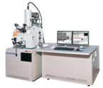
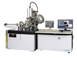
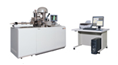
1. Transmission Electron Microscopes (TEM)
 Electron microscopes enable clear observation of micro-structures, which is not possible with optical microscopes. Moreover, they also make it possible to analyze substance structures and obtain atomic level information by using an electron beam. The electron microscope is an epoch-making invention used throughout the world to investigate an atomic world that we could hardly imagine.

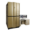
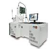
a. JEM-1000 Ultra-High Voltage Electron Microscope
JEM-1000 is the ultra-high voltage (accelerating voltage: 1,000 kV) transmission electron microscope among those used in universities and research institutes worldwide.
Key Features:
- High resolution capability
- High penetration power and thick specimen observation
- Three dimensional observation and in-situ observation experiment
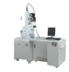
b. JEM-3200FS Field Emission Energy Filter Electron Microscope
The JEM-3200FS Field Emission Electron Microscope is equipped with a field emission electron gun of 300 kV accelerating voltage and an in-column energy filter which shows high performance. This electron microscope offers solutions for various biological and materials researches.
Key Features:
- In-column energy filter (Omega filter)
- New control systems
- New goniometer
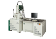
c. JEM-ARM200F Atomic Resolution Analytical Electron Microscope
 JEM-ARM200F is an Atomic Resolution Analytical Electron Microscope, which boasts the world’s highest level STEM-HAADF resolution of 78 pm with a STEM Cs corrector incorporated as standard.
Key Features:
- The world’s highest level STEM-HAADF resolution of 78 pm guaranteed
- Direct observation of atomic column sites of light elements using STEM-ABF imaging
- Atomic resolution analysis with a large solid angle EDS detector
- Observation and analysis with cold FE gun
- TEM Cs-corrector
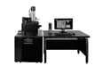
d. JEM-2200FS Field Emission Electron Microscope
 The JEM-2200FS, a state-of-the art analytical electron microscope, is equipped with a 200kV field emission gun (FEG) and the in-column energy filter (Omega filter) that allows a zero-loss image, where inelastic electrons is eliminated, resulting in clear images with high contrast.
Key Features:
- In-column energy filter (Omega filter)
- Control system
- Imaging system
- Piezo-controlled goniometer
- Integration to other instruments
e. JEM-2100F Field Emission Electron Microscope
 The JEM-2100F is a multipurpose, 200 kV FE (Field Emission) analytical electron microscope. Variety of versions is provided to adapt user’s purposes. The FE electron gun (FEG) produces highly stable and bright electron probe that is never achieved with conventional thermionic electron gun. This feature is essential for ultrahigh resolution in scanning transmission microscopy and in an analysis of a nano-scaled sample.
Key Features:
- FETEM, for high resolution observation and nano scale analysis
- Highly stable specimen driving system
- Integration to other instruments
f. JEM-2800 High Throughput Electron Microscope
 JEM-2800 is a versatile TEM/STEM that offers superior usability, while simultaneously achieving high-resolution, high throughput and highly sensitive analysis.
Key Features:
- Wide variety of observation modes, including SEM, suitable for any kind of specimen
- Operating environment supported by Automation and Navigation
- High speed analysis with the large area 100mm2 SDD
- Data management system and report writing support tool
g. JEM-1400Plus Electron Microscope (TEM)
 The JEM-1400Plus is a transmission electron microscope (TEM) developed for application in a wide range of disciplines, from biology to materials researches, such as biological sections, polymers, nanomaterials and …. New environment is optimized for ease-of -use TEM operations with followings.
Key Features:
- New operation panel and LCD screen with touch panel offering simple and ease-of-use operations.
- High-precision camera (8 M pixels) fully-integrated with the PC controlled TEM operation system.
- Off-line viewer software [SightX] enabling to review and edit acquired images on a user’s PC in office.
- A wealth of automated functions, including auto-focus, auto-exposure, and auto-montage.
- New image forming lens system, delivering a magnification of x10, and enabling to acquire an entire mesh image
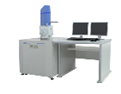
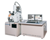
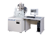
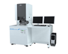
2. Scanning Electron Microscopes (SEM)
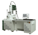 The Scanning Electron Microscope, which is utilized in various fields such as medical, biological, metals, semiconductors and ceramics, is broadening its application frontier. With abundant attachments and devices being combined, its capability is expanding. SEM is regarded as one of the most powerful tools being used at R&D institutes and quality control inspection sites all over the world.
a. JSM-7800F Schottky Field Emission Scanning Electron Microscope
 The newly-developed Super Hybrid Lens (SHL) is used to achieve the next-generation high-resolution SEM, without sacrificing operability. The adoption of the Schottky type electron gun delivers stable analysis with large probe current.
Key Features:
- High resolution observation using the Super Hybrid Lens (SHL)
- Energy selection at low accelerating voltages
- Top surface imaging using Gentle Beam
- Acquisition of all information using multiple detectors
b. JSM-7610F Schottky Field Emission Scanning Electron Microscope
 JSM-7610F is an ultra high resolution Schottky Field Emission Scanning Electron Microscope which has semi-in-lens objective lens. High power optics can provide high throughput and high performance analysis. It’s also suitable for high spatial resolution analysis.
Key Features:
- High resolution imaging and high performance analysis by semi-in-lens objective lens
- The topmost surface imaging at low accelerating voltage by Gentle Beam mode (GB)
- High throughput and high performance analysis by High Power Optics
c. JSM-7500F Field Emission Scanning Electron Microscope
 A field emission SEM with a semi-in-lens and equipped with a Gentle Beam to deliver high-resolution. Of course, a variety of options can be installed, including element analysis.
Key Features:
- Designed for versatility and high resolution
- Gentle Beam (GB) provides top-surface imaging with ultra-low energy incident electrons
- Selective detection of secondary or backscattered electrons with the New r-filter
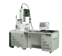
d. JSM-7100F Schottky Field Emission Scanning Electron Microscope
 An easy-to-use, Schottky type SEM with a highly-versatile out-lens and High Power Optics. Based on a user-friendly SEM, combination with attachments of various characteristics, such as observation and analysis at low accelerating high resolution and simultaneous observation of different signals (TTLS system), low vacuum mode (LV system), and observation and analysis with a wide field of view(LDF system), can satisfy the individual needs of each user.
Key Features:
- Highly-versatile Schottky Type SEM
- Order-made FE-SEM
e. JSM-IT300 Scanning Electron Microscope
 In addition to the high image quality observation due to the improvement of the illuminating system, the vacuum system and the signal processing system, the JSM-IT300 is a Scanning Electron Microscope, which can be operated with a high throughput by using touch panel operation and the high speed stage.
Key Features:
- Advanced Functions – Image Quality, Less Charging etc.
- Versatile -Large Chamber and Stage, Analytical Port Geometry etc.
- Intuitive Operation – In Touch Interface, Multi-user/Multi-task etc.
f. JSM-6510 Series Scanning Electron Microscope
 A general-purpose, thermal type SEM to meet the needs of a wide range of users with built-in standard recipes. A wealth of available options, such as Cryo, further expands the range of applications.
Key Features:
- Operation navigation
- Standard recipes
- Wide range of options
- EDS integration
g. JASM-6200 ClairScope Atmospheric Pressure Scanning Electron Microscope
 ClairScope is an instrument to observe specimens by using an Atmospheric Scanning Electron Microscope (ASEM) and an optical microscope. Since specimen remains at atmospheric pressure or in a solution during observation, the original and natural state can be captured.
Key Features:
- Native state (liquid) observation
- Concurrent imaging with an optical microscope
- Dynamic observation
3. Sample Preparation Equipment
a. EM-09100IS Ion Slicer™
 The Ion Slicer can prepare thin-film specimens without solvents or chemicals and requires no prior treatment of the specimen other than rectangular slicing (no disc grinding or dimple grinding).The Ion Slicer prepares thin-film specimens faster and easier than conventional preparation tools. A low-energy, low-angle Ar ion beam irradiates the specimen while a thin shield belt allows low-angle irradiation of the Ar ion beam (from 0° to 6°), drastically reducing ion-beam irradiation damage to the specimen
b. IB-09060CIS Cryo Ion Slicer™
Key Features:
- For easy preparation of TEM thin film/SEM cross section samples of heat sensitive materials
- Minimizes thermal damage during ion irradiation using liquid nitrogen
- Prepares TEM thin film lamella samples and SEM cross section samples*
- Long cryo retention time to fully eliminate damage
- Specimen exchange with liquid nitrogen injected
c. IB-09020CP Cross Section Specimen Preparation Device
d. IB-09010CP Cross Section Polisher
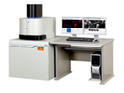
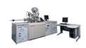
4. Electron Probe Microanalyzer (EPMA)
 The Electron Probe Micro Analyzer (hereinafter, “EPMA”) is an instrument to analyze which elements compose a substance, by irradiating electron beams onto the substance surface and measuring the characteristic X-ray that is generated.
a. JXA-8530F Field Emission Electron Probe Microanalyzer
 JEOL revolutionized surface analysis with an EPMA featuring a field emission (FE) electron gun, and now is proud to present a new upgraded FE-EPMA. The JXA-8530F operates on PC Windows for data acquisition and analysis while maintaining the powerful hardware of the JXA-8500F including the FE electron gun, EOS, and vacuum system to achieve the ultra micro area analysis.
Key Features:
- PC Control
- High spatial resolution in X-ray mapping with the FE electron gun
- Click Point Analysis, User’s Recipes
- Advanced Operation
- Combined WD/ED System
b. JXA-8230 Electron Probe Microanalyzer
 The EDS, which is a versatile and easy-to-use X ray detector, can be mounted. A combined WDS and EDS system provides a seamless and user-friendly environment for analysis. The JXA-8230, designed for user-friendly operations, provides for a complete range of analyses through a new, simple to use, PC-based interface. The high-accuracy and fast speeds offered by the JXA-8230 are a result of its sophisticated hardware developed from JEOL’s EPMA technologies refined over nearly 50 years. The JXA-8230 is powerful, next-generation, analytical tool that fully meets all of the requirements of an EPMA.
5. Auger Microprobe (Auger)
 An Auger microprobe is a very useful instrument for clarifying the various phenomena related to material surfaces. There are many unknown areas in this field, and the obtained information is very interesting by itself. At the same time, it is indispensable for material development.
a. JAMP-9510F Field Emission Auger Microprobe
It is a high specification Auger electron spectrometer with a hemispherical analyzer to provide high throughput analysis of the chemical bonding state at nano to micro areas, and a field emission electron gun also used for EPMA, because it can deliver a large, stable electric current The highly precise eucentric specimen stage makes it possible to perform the previously-impossible analysis of insulators.
Key Features:
- High-sensitivity &high-resolution analyzer
- Schottky Field Emission Electron Gun
- Eucentric Specimen Stage
- Durability
6. Photoelectron Spectrometer (ESCA)
 X-ray Photoelectron Spectroscopy (hereinafter: XPS) has been used as a highly versatile analytical method in the research and development of materials, and for quality control. The photoelectron spectrometer is used in a wide range of applications, from Universities to factories, as a research tool with ease of operation that enables routine analyses.
a. JPS-9200 Photoelectron Spectrometer
 This is a high-sensitivity photoelectron spectrometer for general application, with a wide analysis range from 3µm&phi to 3mmφ.
Key Features:
- Micro Ion Gun
- Hybrid Input Lens System
- Data analysis software for surface analysis
b. JPS-9010 Photoelectron Spectrometer
 A well-balanced multifunction photoelectron spectrometer equipped with high-speed etching gun and twin anode monochromator, which also realizes low cost.
Key Features:
- Kauffmann Type Ion Gun
- Pan Focus Input Len System
- Data analysis software for surface analysis
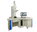
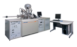
7. MultiBeam (SEM-FIB)
MultiBeam is a new high performance SEM and micro milling FIB, combines the most popular LaB6 electron column in the world with real time milling and monitoring capability.
a. JIB-4601F MultiBeam System
 The JIB-4601F is a MultiBeam processing and observation system that incorporates a Schottky-type SEM and a High-Power FIB column. After performing cross-section milling of a region using FIB, it is possible to observe and analyze the internal portions using SEM. The FIB can be used for fine milling and TEM sample preparation, as well as performing 3-dimensional structure analysis with automatic cross-section milling/ observation & analysis at fixed intervals. The Schottky-type SEM enables easy positioning of the target site, as well as observation and analysis of minute structures.
b. JIB-4501 MultiBeam SEM-FIB System
 The JIB-4601F is a MultiBeam processing system that incorporates a thermionic SEM and a high-performance ion column. The instrument can be used as a SEM system to observe specimen surfaces; or section milling of milling of a region using FIB can be performed, followed by element analysis and observation of the internal portions using SEM. The FIB can be used for fine milling and TEM thin-film sample preparation. The large chamber expands the possible range of applications. A low-vacuum mode enables SEM observation without any coating of insulating material, so it can be used in almost any field
c. JIB-4000 Focused Ion Beam Milling & Imaging System
 The JIB-4000 is a focused ion beam processing and observation system (single-beam FIB system) featuring a high-performance ion column. The accelerated Ga ion beam is focused and applied to the sample to enable SIM image observation of the sample surface, milling, and deposition of materials like carbon or tungsten. It is also possible to fabricate cross-section samples in order to observe the sample interior or thin film specimen for TEM imaging. In comparison to a SEM image, a SIM image shows noticeable channeling contrast due to differences in the crystal orientation
8. X-ray Fluorescence Spectrometers (XRF)
9. Nuclear Magnetic Resonance
Nuclear magnetic resonance is a physical phenomenon in which nuclei in a magnetic field absorb and re-emit electromagnetic radiation.
a. JNM-ECA Series FT NMR
 The JNM-ECA series is an FT NMR spectrometer developed making full use of the latest digital and high frequency technology. This high performance, sophisticated spectrometer designed to take advantage of high field magnet development to include 1GHz. Innovative features to support not only the conventional NMR applications such as structural analysis of molecules and evaluation of materials but also future progress of science and technologies including research for development of new drugs, postgenome research and development of new materials.
b. JNM-ECX Series FT NMR
 The JNM-ECX series is an FT NMR spectrometer developed making full use of the latest digital and high frequency technology. This high performance, sophisticated spectrometer designed to take advantage of high field magnet development to include 1GHz. Innovative features to support not only the conventional NMR applications such as structural analysis of molecules and evaluation of materials but also future progress of science and technologies including research for development of new drugs, postgenome research and development of new materials.
c. JNM-ECS Series FT NMR
 The JNM-ECS series is a compact two-channel spectrometer that retains the advanced capabilities of the ECA spectrometer. The required installation space is reduced by one-half when compared to conventional NMR spectrometers. When installed in combination with the optional new generation super shielded superconducting magnets (SCM), the installation layout is very flexible.
10. Electron Spin Resonance
Electron spin resonance (ESR) spectroscopy is a technique for studying materials with unpaired electrons. The basic concepts of EPR are analogous to those of nuclear magnetic resonance (NMR), but it is electron spins that are excited instead of the spins of atomic nuclei. Because most stable molecules have all their electrons paired, the EPR technique is less widely used than NMR.
a. JES-FA Series ESR
 JEOL RESONANCE’s ultrahigh sensitivity ESR instrument is offered as a fully computer controlled model with a new magnetic field control system built-in. The JES-FA ESR can be used for any ESR measurement ranging from routine to more specialized research activities. The JES-FA series is so easy to use that it will become your partner in the laboratory
11. Mass Spectrometers
The mass spectrometer is an instrument which can measure the masses and relative concentrations of atoms and molecules. It makes use of the basic magnetic force on a moving charged particle.
a. JMS-S3000 Matrix-Assisted Laser Desorption/Ionization Time-of-Flight Mass Spectrometer
 The JMS-S3000 is a MALDI-TOF MS incorporating JEOL’s unique Spiral TOF ion optic system. Featuring unprecedented levels of mass resolution and sensitivity, the system has been acknowledged for its distinctive capabilities in many scientific studies.
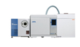
b. JMS-T100GCV High Performance Gas Chromatograph – Time-of-Flight Mass Spectrometer
 AccuTOF™ GCv 4G with high speed, high resolving power and high mass accuracy. These are chromatograms of 100 pesticide components. In the Fast GC analysis (top right), the system acquired data while maintaining chromatogram separation in less than 1/4 of the time needed for the conventional analysis. The 50 spectra/second high speed data acquisition system enables high throughput analysis.
c. JMS-Q1050GC Master-Quad GC/MS
 Key Features:
- Wide Dynamic Range : Responding to a wide range of sample concentrations
- High Sensitivity : Stable for a long period of time – High Evacuation Performance : Enabling analysis under severe acquisition conditions
- Maintainability: Fast and easy “Escrime™”: Enabling to analyze a multi-component sample at one time.
- Extensive GC-MS solutions : Proposing a broad range of systems
d. JMS-T100LP LC-TOFMS
 A versatile TOMFS fulfilling every analytical need with one unit. Depending on the research purpose, selection of various ion source is possible.Standard equipment of an isolation valve and dry nitrogen tank has realized an LC-TOFMS that is easier to maintain. In addition, the optional Cold Spray Ion Source* is especially powerful for the observation of unstable compound bonded by weak forces, such as hydrogen bonds which has been difficult with conventional ESI ionization methods.
e. DART Direct Analysis in Real Time
 DART is a new ion source that allows for non-contact, rapid analysis of samples at atmospheric pressure at ground potential under ambient conditions.DART is a dedicated ion source for the JMS-T100LC/LP/CS, high-resolution time-of-flight mass spectrometers (AccuTOFTM™). The DART-AccuTOF™ combination permits exact estimation of elemental compositions based on exact mass measurement
f. JMS-700 MStation Mass Spectrometer
 A high resolution mass spectrometer featuring full-control by computer, equipped with auto-tuning of various parameters including the ion source
g. JMS-800D High-Resolution Mass Spectrometer
 JMS-800D UltraFOCUS™ is an instrument focusing on ultramicro analysis, which is optimal for dioxins in HRGC/HRSIM mode, as well as the related compounds of PCB, PBDE, and POP compounds
To get more details on the mentioned products, call +965 1805151 or email at sel@ashraf.com